Making the Cut
By Fenella Saunders
Japanese paper arts are inspiring materials scientists with new ways to turn flat sheets into functional devices.
Japanese paper arts are inspiring materials scientists with new ways to turn flat sheets into functional devices.

DOI: 10.1511/2015.117.375
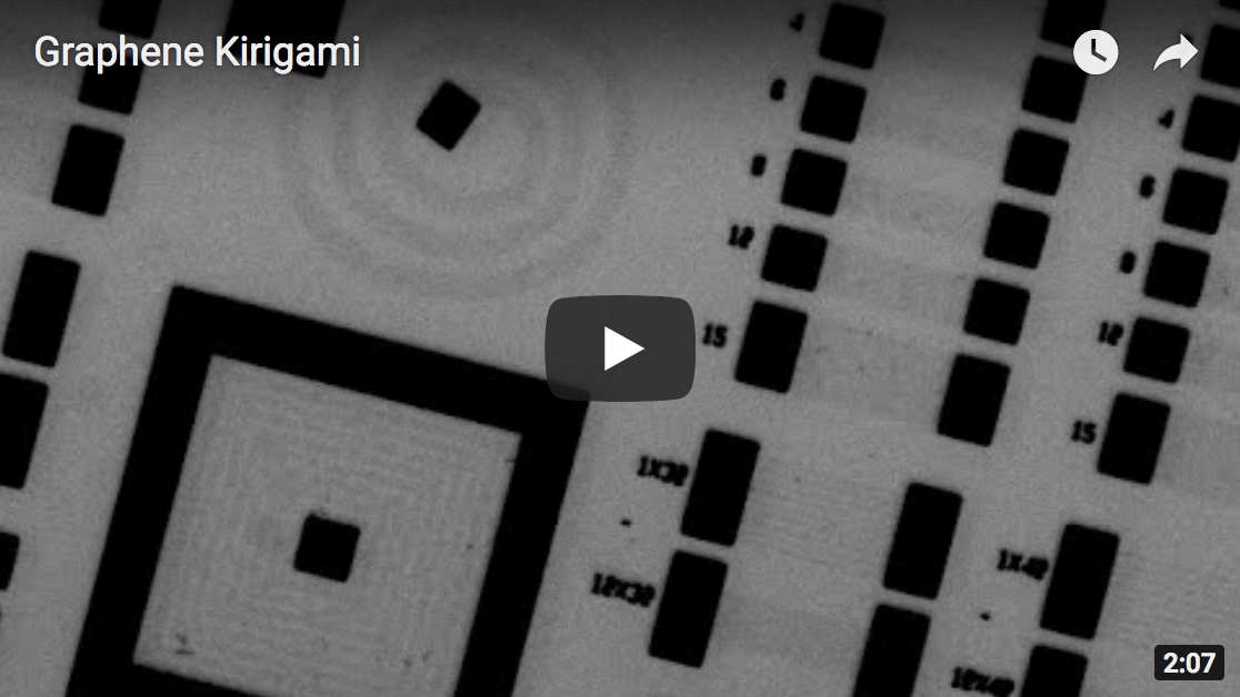
Paul McEuen, a physicist at Cornell University, was looking for an interesting project for his graduate student Melina Blees, who also has artistic skills. “She had been studying minute detail of an electronic device made out of graphene and carbon nanotubes, and honestly, it was kind of killing her soul,” says McEuen. Nanotubes are lattices of carbon atoms that are rolled up into a cylinder; graphene is the same basic atomic arrangement, but unrolled into a flat sheet. “This idea came up that we have this atomic scale paper, why don’t we try to do paper arts with it.” McEuen, Blees, and their colleagues have since used techniques from Japanese paper-cutting artwork to create microscopic, functional three-dimensional devices from graphene. “From those humble beginnings, it’s become a major research thrust for us and other groups,” McEuen says.
McEuen and his group have created simple structures, such as hinges and springs, using strategic patterns of cuts. They have bent and stretched these devices thousands of times without damage. Folding sequences could be triggered by physical pushing, or magnets and chemical signals; strands of DNA-based “glues” might be used to control binding and hold them in place, McEuen says. The graphene can be layered with other materials, such as electronic components. For instance, McEuen says they are starting to use the stretch in a graphene spring to measure the electrical signals from neurons. They are also working on microscopic containers that could release their contents on cue.
Inspiration from paper cutting (called kirigami) and folding (origami) has recently hit several researchers, working across large ranges of size scales. John A. Rogers, a materials scientist at the University of Illinois at Urbana-Champaign, and his colleagues are also interested in integrating 3D devices with biological systems, but they want to work with materials such as silicon that are found in high-quality electronics, and are inherently brittle.
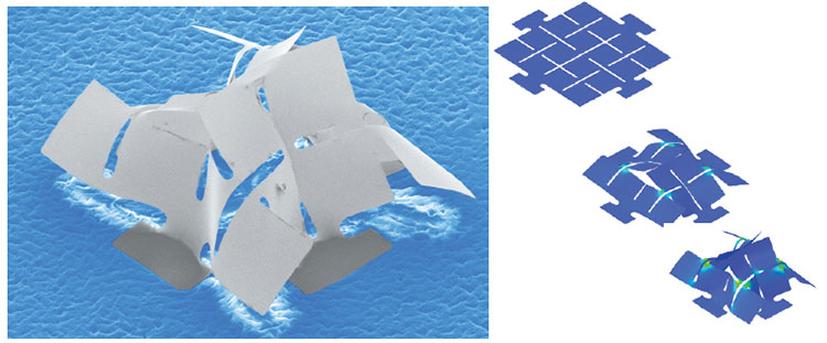
Images courtesy of John A. Rogers.
Rogers and his team design complex series of cuts into silicon membranes, which are layered onto a prestretched rubber sheet. Engineered surface chemistry between the silicon and rubber causes the material to buckle in a controlled sequence as the tension in the rubber is released, to create elaborate, tiny structures. “If you didn’t have the cuts there, the material would just break if you applied these compressive forces and attempted to do this 3D transformation,” Rogers says.
One of the uses that Rogers and his team are exploring for these structures is to observe, and maybe someday control, cellular behavior. “We’re growing cells on top of these things; it’s sort of like a cellular-scale jungle gym,” he says. “The scaffold can measure cellular-level activity, proliferation, death, and differentiation, and perhaps produce stimulation patterns to control development of tissue.”
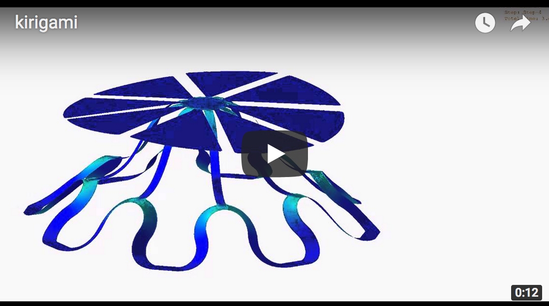
A computer model of one of Rogers' pop-up structures is below:
Silicon, electrical components, and art again combine in kirigami-inspired work by materials scientist Max Shtein and his colleagues at the University of Michigan, but this time on the meter scale. Their group is focusing on photovoltaic cells and developing better ways to have them track the Sun. Current motorized tracking systems are expensive and heavy, so they aren’t used on residential rooftops. Using a flexible, thin film for the solar array, and a series of offset, parallel cuts, the team found that when they stretched such a panel a bit like an accordion, the individual sections between the slits would tilt. Controlling the amount and direction of tilt allows the panel to track the path of the Sun and increase energy-conversion efficiency by more than 35 percent. “We’ve tried a few patterns and this one is an interesting combination of being simple to produce and having really good energy output,” Shtein says.
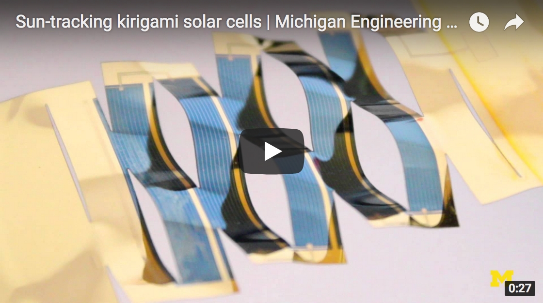
The functionality of these materials might come full circle and feed back into the artistic realm of their original inspiration. Solar cells could be installed in many more places because of their new forms, says Shtein: “The various new aesthetic qualities of our shapes means they could begin being integrated into building facades and other architectural elements, such as window shades, shelters, or sculptures.”
Click "American Scientist" to access home page
American Scientist Comments and Discussion
To discuss our articles or comment on them, please share them and tag American Scientist on social media platforms. Here are links to our profiles on Twitter, Facebook, and LinkedIn.
If we re-share your post, we will moderate comments/discussion following our comments policy.