The Challenge of Manufacturing Between Macro and Micro
By Robert J. Wood
Classic ways of folding paper into dynamic shapes—origami, pop-up books—inspire methods to engineer millimeter-scale machines.
Classic ways of folding paper into dynamic shapes—origami, pop-up books—inspire methods to engineer millimeter-scale machines.

DOI: 10.1511/2014.107.124
Building a complex consumer product like a smartphone involves solving a lot of different engineering challenges. One of the most difficult yet unappreciated is the challenge of scale.
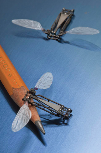
Image courtesy of the author.
A smartphone contains components with sizes ranging from centimeters (the case and screen) to submillimeter (the accelerometer parts that tell the phone which way it is pointing) to submicrometer (the transistors in the processor). Each length requires a different set of materials and a distinctive set of assembly techniques. The final “nuts-and-bolts” creation of the complete phone is possible only after solving the whole set of scale-related challenges.
The large-scale design is what consumers notice most about the finished product and the microelectronics tend to get the most attention in technological discussions. But methods for building things at intermediate scales are actually the least developed. For reasons based on both physics and practicality, techniques used in macro-scale machining and assembly are inappropriate for complex devices with millimeter-scale features. On the other hand, integrated circuit-derived approaches are too limiting in terms of geometry and material choices to create a diversity of millimeter-scale machines. This size range, with features between tens of micrometers to tens of centimeters, is called the meso-scale.
My colleagues and I are developing novel techniques that could allow more flexible and more efficient manufacturing at those intermediate dimensions. One of the most promising directions is a process that sprang from a surprising inspiration: children’s pop-up books. We use some creative techniques to keep all the pieces in these devices aligned during manufacturing, and we employ some intricate joints and scaffolding to automatically fold flat designs into complex geometries.
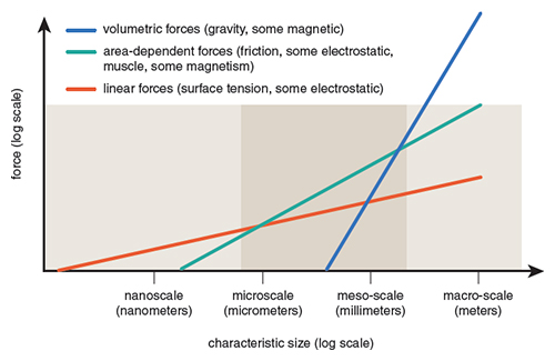
To get to the meso-scale, we have to first understand how a device will operate as its size is reduced. A typical exercise involves analyzing the forces it will experience. For example, when all dimensions scale equally, if one dimension decreases by a factor of 10, volume decreases by 1,000. Therefore, the force from gravity (which is related to mass) is also reduced by 1,000. However, the force from friction with surrounding objects will only decrease by a factor of 100 because it is dependent on area. As objects get smaller, therefore, surface forces such as friction begin to matter much more than gravity does. A consequence is that, say, the kinds of rotary bearings used to create smooth motion in axles and wheels become more and more inefficient due to friction as the scale is reduced. The combination of reduced efficiency and the challenges of manufacturing at small scales has motivated alternatives for movement that are instead based on bending, like hinges. A similar scaling analysis can be done for fluid forces, electromagnetic forces, electrostatic forces, and surface tension.
Barbara Aulicino
Just as forces and effective mechanisms change with scale, so do practical manufacturing methods. To create meso-scale devices, we first examined the viability of scaling down existing macro-scale processes, and the combination of some of these methods into new processes.
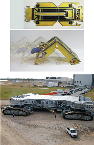
Top two images courtesy of Sam Felton; bottom image Wikimedia Commons
Manufacturing methods that create structures by depositing or adding layers of material are called additive processes. One prominent example is 3D printing, and it has evolved tremendously over the past few decades in both research and commercial environments. Commercially available printers use a variety of materials and methods, from the setting of heated wax to inkjet-style printers that extrude ultraviolet- curable polymers, to stereolithography systems (which uses an ultraviolet laser to cure layers of liquid resin) and lasers that selectively sinter powder into a solid form. Such systems have dramatically reduced the barriers to entry for generating three-dimensional parts—and even articulated mechanisms can be created in one print without assembly.
The primary drawbacks for commercial 3D printers are the cost of raw materials and material quality. Most printers are limited to either a single material or a single type of material (usually polymers). Regardless of these limitations, 3D printers have achieved widespread adoption both for prototype development in industry and as an invaluable educational tool in academia. More recently, the “maker” movement—a subculture that encourages everyday people to invent and create—has democratized access to 3D printers by creating low-cost versions of the devices. 3D printers are nearly affordable for home use and are following a similar price and adoption trend as the now ubiquitous 2D printers in nearly every home and office.
Research in 3D printing has focused on expanding the variety of printable materials and exploring the limits of scalability. Expanding material diversity is a critical step toward monolithic printed devices—ones that include all their components without any additional assembly. New high- performance polymers, printed conductors, and even complete batteries have been demonstrated recently. With respect to scaling, one example of commercially available micro-scale 3D printing is two-photon lithography, which uses lasers to directly write 3D patterns in a polymer. Submicron resolution is possible, but at the expense of build time for structures with centimeter or larger size scales.
For any additive process that builds structures layer by layer, position errors in each step will integrate over the course of fabrication.
Alternatives to additive manufacturing where materials are directly deposited include molding and casting. Such processes have benefits for inexpensive mass-produced components, yet for submillimeter scale, they still require specialized tooling to create the mold. One exception is soft lithography, which grew out of research in microfluidics, where microscopic channels are used to transport tiny quantities of fluid, the basis for devices such as inkjet printers and DNA-analyzing chips. Soft lithography leverages a range of tools borrowed from integrated circuit fabrication, with an added emphasis on the use of surface properties to create layered devices. First the integrated-circuit technique of photolithography is used to pattern a photoresist—for example, a pattern in a layer of material is cured by light and the uncured sections are chemically etched away. In this case the photoresist is used as a mold to create features in a flexible polymer or as a stamp for subsequent contact-based material deposition.
The process is inherently cheap: It requires a few tens of dollars worth of materials, a transparency mask, minimal (and common) lab equipment, and modest specifications for cleanliness (compared to integrated circuit production). However, soft lithography results in quasi-two-dimensional devices; to construct 3D structures requires methods for aligning and bonding multiple layers, which could increase cost, complexity, and process time. Also, for any additive process that builds structures layer by layer, position errors in each of the deposition iterations will integrate over the course of fabrication. This concern requires either high-fidelity position feedback, or the device must be able to withstand increased errors as the number of layers in a build is increased.
An alternative to building up devices is to carve them out of a larger piece, so-called subtractive processes. At the macro-scale, milling machines can have a repeatability and precision on the order of 1 micrometer. However, it’s uncommon to find milling tools to below 100 micrometers in diameter. To go smaller, to the meso-scale, requires switching to noncontact machining methods, such as lasers, high-pressure water, or electrical discharges (where a spark between two electrodes does the cutting).
A number of single folds that simultaneously happen is the enabling innovation for our process inspired by pop-up books.
Laser machining is now common and has characteristics appropriate for meso-scale devices. There are many laser properties that determine cut quality and suitable materials, but the most important parameters for machining are wavelength, pulse duration, and repetition rate.
Wavelength is a determinant for the types of materials that can be machined, and it can range from a few hundred nanometers in ultraviolet to 10,000 nanometers in deep infrared. Long wavelengths have two consequences: larger spot sizes and thus larger minimum feature sizes, and limits on the types of materials that can be machined. Wavelengths in the infrared range produce more heat and are better suited for machining materials with low thermal conductivity, such as polymers and organic materials. Some metals can also be machined with infrared lasers if the power is sufficiently high. However, its use becomes impossible for metals with very high thermal conductivity, such as aluminum.
Ultraviolet lasers are capable of ablating a wider range of materials, including metals, semiconductors, and fiber-reinforced composites with spot sizes on the order of 1 micrometer. Lower wavelengths put more energy into breaking chemical bonds as opposed to heating the material, generally resulting in cleaner cuts with minimal damage to the surrounding regions. The downside with ultraviolet lasers is primarily due to high cost.
Pulse duration and repetition rate affect the speed of cutting and quality of the cut. Lasers are available that operate in pulses from femtosecond duration to continuous wave. In general, for the same energy per pulse, the lower the pulse duration, the cleaner the cut because there is less time for heat convection. Faster repetition rates result in faster cutting, but speed is also limited by the beam delivery system and how fast it moves over the target.
Water jets—where a high-pressure stream is pushed through a small nozzle to create a forceful cutting tool—can process most of the same materials as lasers, and the finest resolutions available are on the order of tens of micrometers. “Micro” electrical discharge machining processes can also produce feature sizes of approximately 10 micrometers, but are constrained to conductive materials. However, the range of metals available to electrical discharge machining includes hard or hardened metals that are difficult to cut with more conventional subtractive methods.
Both additive and subtractive processes have their limitations, but they are not mutually exclusive, so there are ways to use both. This combination is particularly important for micro- and meso-scale manufacturing and assembly given the challenges of scaling down “nuts-and-bolts” methods. A monolithic procedure is needed where all electrical and mechanical functionality is embedded in a single device, without manual assembly.
Images courtesy of Sam Felton.
Printed circuit boards are a prime example. Although often thought of as purely a substrate for electrical systems, modern boards are highly engineered composites that have complex electrical, mechanical, and thermal characteristics. Printed circuits are often many tens of layers thick with electrical vias—vertical conduits that connect any two layers in the stack. Both additive and subtractive processes are needed to make these complex composites.
Another example is shape deposition manufacturing. This process follows a cycle of deposition—typically by molding thermoset polymers—followed by machining. This cycle can be repeated indefinitely to incorporate more materials or more complex geometries, resulting in 3D composites and flexure-based articulated mechanisms. One of the primary benefits of this method is the ability to encapsulate discrete electromechanical components—such as sensors, actuators, or electronics—within the device during any of the molding steps.
Finally there are microelectromechanical systems, or MEMS for short. Devices in this regime range from 20 micrometers to 1 millimeter. They are built using procedures derived from fabricating semiconductor devices, and combine surface and bulk machining for material removal and iterative material deposition steps. By bonding together whole silicon wafers of the type usually used to build microchips, it is possible to create layered devices. Although there have been significant advances in high aspect ratio micromachining techniques, MEMS remains a mostly planar process. To overcome the “2.5D” nature of most MEMS processes, researchers have developed ingenious ways of constructing hinges from layers of surface micromachined polycrystalline silicon. This advance represents some of the first uses of folding to create more topologically complex mechanisms at the millimeter scale. But my colleagues and I came to realize that folding has far more potential.
In our laboratory, my colleagues and I saw that folding has many possible benefits over other assembly methods, such as the potential for single piece construction and the relative simplicity of 2D machining methods. In addition, folded beams—which may act as structural components in devices—use material efficiently and have high stiffness-to-weight ratios compared to solid beams. Furthermore, starting from a quasi-2D sheet trivializes the integration of electrical components as it becomes possible to use standard pick-and-place printed circuit board assembly tools.
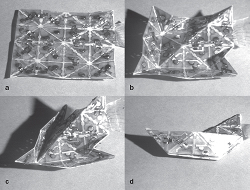
Image courtesy of the author.
In fact, printed circuit boards themselves are not limited to 2D structures. Thin polyimide-based flexible circuits are now ubiquitous as folded components in modern electronics. Some of these components are designed to fold just once, such as to make a board fit into an irregular shape such as in the smartphone example above. In other cases, the flexible parts can move repeatedly, such as in the read-write circuit in a disk drive. To date, these folds have been serial folds, with one step following another, like folding a paper airplane. An expansion of this to parallel folds, where a number of single folds simultaneously happen at different points on the device, is the enabling innovation for our process inspired by pop-up books. This innovation came about by necessity—researchers in my group were making small robots by folding, but performing the assembly by hand was tedious and lacked repeatability. In conversations with two of my then-graduate students, Pratheev Sreetharan and Peter Whitney, we decided that there must be a better solution—one that mirrored the complexity of the folded structures that appear in children’s pop-up books and was created with similar ease (i.e., a simple turn of the page pops everything into place).
One obvious question is how much diversity of shape we can create just by folding. Fortunately, computer scientists have proven that any polyhedra can be folded out of a single continuous sheet of paper. Furthermore, by controlling the specifications of the polyhedra, we can create nearly any linkage mechanism. The only obvious limitation in creating mechanisms purely by folding is the lack of continuously rotating joints—flexures have a finite range defined by geometry and material properties.
Origami-like techniques have been used to create intricate sculptures with thousands of folds, but they require many hours of work by hand. Similar folding mechanisms have been shown to be ubiquitous in nature, from the folds in protein structures to the unfurling of leaves and insect wings when they first emerge. There are also myriad applications in engineered systems, including parachute packing, unfolded solar panels on satellites, and quick-deployable shelters. For engineered systems, alternatives to tedious hand folding include the use of pneumatics or hydraulics to expand and shape devices, and also the use of materials with shape memory that will return to their original shape even after being confined. But part of the challenge is making it work at the scales useful to manufacturing, particularly at the meso-scale.
Another important question for assembly by folding is how to design folded structures and mechanisms. Origami has historically lived in the realm of art, and the most impressive pieces have come from a small number of highly experienced, talented individuals—not a practical source for rapid machine design. There has been progress in creating design tools that generate fold patterns automatically given a 3D geometry. But such tools are not currently at the same level as those for established procedures, such as integrated circuit fabrication.
A final potential challenge is not just in the creation of static folded structures (i.e. structures incapable of movement) but in designing articulated mechanisms that can be assembled by folding. This requires two types of folds: static assembly folds used to define geometry and structural properties, and dynamic folds that are flexures used to constrain motion along desired axes. This goal is a further challenge for design automation tools, potentially involving highly complex kinematics (and it could be even more difficult to define the inverse kinematics that would “unfold” the device into the 2D crease patterns necessary for fabrication by folding).
Inspired by the capabilities of folding, and drawing techniques from the best additive and subtractive processes, over the past few years we have developed a new manufacturing paradigm called pop-up book MEMS. The process consists of three steps: bulk micro- or meso-machining, lamination, and automated assembly by folding. The first step cuts patterns into thin (between 1 micrometer and several hundred micrometers) material sheets by any noncontact machining method—but we typically use ultraviolet lasers because of their material nonspecificity, speed, and minimum feature sizes. Unlike other processes, any material can be included: metals, polymers, ceramics, and composites.
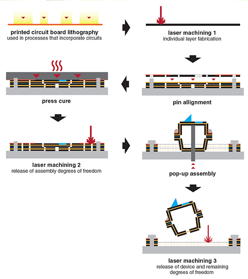
Barbara Aulicino
The second step laminates all the constituent material layers into one quasi-2D composite sheet. This is made possible by two aspects of the first step: Not only are the functional layers machined, so are free-standing film adhesives that serve to bond the layers together. In addition, holes are cut in each layer during the first step to allow the use of pins for alignment during lamination. Persistent pin alignment during curing solves the problem of spatial errors that accumulate when adding more layers. These first two steps share many similarities to multilayer printed circuit board assembly.
The final step folds the 2D composite into the desired 3D structure or mechanism. This step is done in a fundamentally different way than serial origami folds or flexible circuit boards. Instead we draw inspiration from the parallel folds in children’s pop-up books, which assemble complex geometries using a single direction of movement (created by opening and closing the book). This parallelizes construction, eliminating the need for skill-based serial construction that is characteristic of most factory floors, and breaks away from the limitations of both additive and subtractive assembly processes. It also advances the assembly from being done by hand under a microscope (perpetuating the “graduate student with tweezers” paradigm).
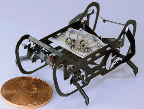
Image courtesy of Andrew Baisch.
A central structure in pop-up assembly are mechanical vias, similar to electrical vias in multilayer printed circuit boards, which connect any two layers to each other. The film adhesives used to assemble layers in these devices are free standing and also possible to machine. A typical substructure of the entire composite consists of outer rigid layers sandwiching a thin, flexible polymer, and bonded with adhesive layers. Gaps in the outer composite layers—exposing the thin polymer—result in flexible joints entirely contained within the thickness of the laminate, which can be folded into static structures or articulated mechanisms. Any number of these linkage layers can be composed to create arbitrarily complex mechanisms.
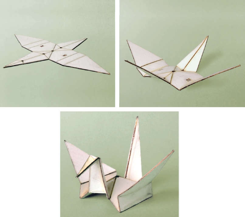
Image courtesy of Pratheev Sreetharan.
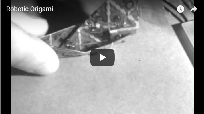
One example of the complexity we can achieve with this process is illustrated by the assembly of a RoboBee prototype. In this example, the functional components of the RoboBee are created simultaneously with an assembly scaffold that controls the motions of all the components during assembly. Pins pushing up from under the bottom level unfold flexure-based linkages that lift the top scaffold, which in turn activates other mechanisms to fold the device into shape. Connecting several linkages creates complex movements, so that, say, part of the device can remain level while other pieces fold upward. The assembly, still attached to the scaffold, is immersed in a bath that electroplates metal points on the device, locking it in shape so that it can be removed from the scaffold. (A video of the process is below.)

The pop-up book MEMS process has multiple benefits. First, because we are machining each layer individually, and then bonding using a separate adhesive, we can use any material combination (as long as we choose an adhesive that is compatible with all materials). Fiber-reinforced composites can be used for high stiffness and low weight. Electroactive materials can be used to create sensors or actuators. Biocompatible materials can be included for medical applications.
Images courtesy of Kevin Ma.
Second, the process is inherently scalable, both up and down. To date we have used an ultraviolet laser with a roughly 10 micrometer spot size. However, given a finer laser spot size, or an alternative 2D micromachining method, this limit could be significantly reduced. At smaller feature sizes, the free-standing film adhesives would be difficult to machine, so we might have to employ other bonding methods such as liquid adhesives.
Third, structures with any geometry and mechanisms with any number of degrees of freedom are able to be assembled by folding. The only limitation is the lack of a freely rotating joint, but even this restriction could be eliminated (if friction were not a concern) by choosing the appropriate layup and geometry to create rotary bearings in the laminate.
Finally, the process is inexpensive, due partly to the lack of substantial infrastructure required to carry out the process steps. Furthermore, the manufacturing aspects of the process are very fast. Complete electromechanical systems can be created in hours and multiple copies can be arrayed either in the plane of the laminate or stacked on top of each other, which outlines a natural avenue to mass production.
The origin of the pop-up book MEMS process is rooted in the assembly of microrobots such as the Micromechanical Flying Insect, a robotic microflyer inspired by house flies, which was designed by Ron Fearing’s group at the University of California, Berkeley. Its goal was to be at most 25 millimeters in diameter and to hover under its own power. From the early stages of the robotic-insect project in the early to mid-2000s, it was clear that neither MEMS nor macro-scale manufacturing methods were well suited for the mechanisms, structures, and actuators required to achieve flight with a robot the scale of a housefly. Laminated or folded beams were chosen for structural members, and articulation was achieved with compliant flexures. But again, all the folding was done by hand. There was a more subtle disadvantage to this process as well—difficulty in assembly and poor repeatability caused robot developers to be conservative in their designs.
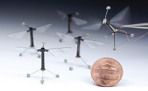
Image courtesy of Kevin Ma and Pakpong Chirarattananon.)
The pop-up book MEMS process partly fulfills legendary physicist Richard Feynman’s prophesy, made in his 1959 lecture “Plenty of Room at the Bottom,” regarding little robots building even smaller robots. For example, after the Micromechanical Flying Insect, we began the RoboBees project, for which we have been able to construct monolithic robots in one or two assembly steps (depending on the complexity of the design) where the scaffold acts as the tiny hands that piece together the parts of the robot. This example takes advantage of many of the benefits of pop-up manufacturing: Complex structures and articulated mechanisms are created with minimal dexterous manipulation of the constituent components; electroactive materials are included directly in the layup, resulting in the “flight muscles” for the robot; and the laminate consists of a variety of materials.
Structures and mechanisms with any number of degrees of freedom can be assembled by folding.
Recently the scope of devices created using the pop-up book MEMS process has been dramatically expanded. Examples include flying and terrestrial insect-like robots that could quickly survey disaster areas or perform environmental monitoring, as well as surgical devices, new meso-scale actuators, bio-inspired sensors, and a host of polyhedra and parallel mechanisms that would be difficult or impossible to build by other means.
These advances in meso-scale manufacturing have opened the door to countless applications in consumer electronics, biomedical devices, on-demand tooling, and research and education. But there are still many barriers to widespread use. Infrastructure costs and design expertise still make many of the methods discussed here a challenge for novice users.
Clues to the solution to more universal access to meso-scale manufacturing come from the history of integrated circuits. Early in their development in the 1980s, the U.S. National Science Foundation and Department of Defense funded a service called MOSIS (Metal Oxide Semiconductor Implementation Service) that acted as a gateway to multiple integrated circuit foundries. Small amounts of wafer real estate on well-defined integrated circuit fabrication processes were made available to any researcher. Thus researchers could generate prototypes with minimal expense (compared to the cost of a full run, or investing in the infrastructure themselves) and with highly refined process standards, the details of which could simply be abstracted away by their design tools.
As the MOSIS service evolved, so did the design tools that automated common features and generally made it easier for novice users to generate new designs and intellectual property. Beyond the obvious benefits the service provided in terms of access to fabrication, MOSIS also generated a vibrant community of users that in turn pushed the limits of the processes, developed and disseminated new designs and design rules, and generally built up an intellectual foundation that pushed the proliferation of electronic devices that are now integral in our daily lives.
A similar trajectory could equally aid developers of multiscale, multimaterial, monolithic electromechanical devices. Given the relatively low infrastructure costs for processes such as pop-up book MEMS, and with the motivation to establish standardized process lines, there is a huge opportunity to establish a MOSIS-like system that will make the process accessible. But the foundry and processes alone would not be enough. Design rules and automation tools, such as computer-aided design software, must be published simultaneously.
One of the more intriguing consequences of a cheap, flexible monolithic manufacturing system is that it could inspire a rich user community, appealing to the fast-growing “maker” movement. Like the electronics hobbyists who started tinkering with integrated circuits starting in the 1970s, today’s makers may prove vital for building up design libraries and for finding novel applications of pop-up assembly. In a few decades, perhaps people will be manufacturing their own small robots as easily as they now print their digital photos.
Click "American Scientist" to access home page
American Scientist Comments and Discussion
To discuss our articles or comment on them, please share them and tag American Scientist on social media platforms. Here are links to our profiles on Twitter, Facebook, and LinkedIn.
If we re-share your post, we will moderate comments/discussion following our comments policy.