Fabrication at the Nano Scale with Molds and Imprinting
By Jaslyn B. K. Law
Technologies similar to embossing can now be used at minuscule sizes to mechanically create novel devices.
Technologies similar to embossing can now be used at minuscule sizes to mechanically create novel devices.

DOI: 10.1511/2015.114.212
Over the next few decades, growth in the field of nanotechnology is predicted to be similar to that of the early days of the computer revolution in the 1970s.
This ultra-miniaturization process works at length scales of around 100 nanometers and below; 1 nanometer is about a 50,000th of the width of a hair. Materials behave differently at the nano scale, and exploiting these properties can lead to advances in everything from computer chips to medical treatments. But many of the traditional fabrication methods aren’t precise enough to work at these scales, so researchers have taken inspiration from history to develop new material patterning methods.
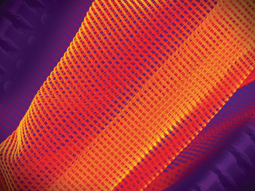
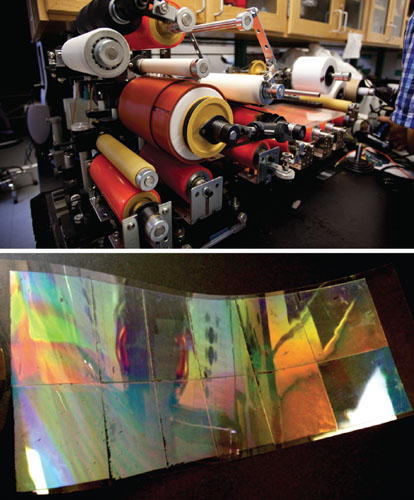
Image courtesy of Debashis Chanda, NSTC/CREOL, University of Central Florida; and John A. Rogers, MSE, University of Illinois at Urbana-Champaign.
In 1959, physicist Richard Feynman seeded the concepts of nanotechnology in his seminal lecture “Plenty of Room at the Bottom,” but the actual term was coined by Norio Taniguchi of the Tokyo University of Science in 1974, where he described the key idea of nanotechnology as “the processing of separation, consolidation, and deformation of materials by one atom or by one molecule.” It was not until the 1980s, with the advances in microscopy (particularly the invention of the scanning tunneling microscope), that scientists could study matter organized at the nanoscale, as a bridge to commercial production.
The past two decades have witnessed the development and great advancement of a variety of nanofabrication techniques. Generally these techniques can be classified into two main categories: top-down and bottom-up approaches. Top-down nanofabrication can be likened to the process of sculpting from a block of stone, cutting away unwanted material from a blank base. Bottom-up nanofabrication can be visualized like the process of building a brick house, creating a structure piece by piece.
The goal of nanofabrication is to create commercial products, so to be successful in going from a laboratory proof-of-concept prototype to high-volume manufacturing, a process technique must be flexible, reliable, up-scalable, and cost effective. Bottom-up approaches still suffer from several of these technological challenges, including the ability to precisely position pieces, which affects flexibility and reproducibility. On the other hand, there are two top-down approaches that have already been shown to work well. One of these, optical lithography, is well established—it’s the standard process used to make computer chips. The other, nanoimprint lithography, is an emerging technique for mechanically patterning materials with great precision. My colleagues and I use the latter technique to pattern polymer films with nano scale structures that give them new optical and physical properties.
Optical lithography was introduced in the 1960s and remains the dominant patterning technique for semiconductor computer chips, although the patterning resolution has significantly advanced. A semiconductor chip is made up of many layers, each with a different geometry that requires precision alignment to the previous layers. The process uses light to translate circuit designs from a mask into patterns on a silicon wafer coated with a light- sensitive polymer called a photoresist. There are two types of photoresist; each undergoes a different reaction after light exposure and subsequent treatment with a chemical called a developer. If a positive photoresist is exposed to light, it becomes soluble to the developer and is washed away, leaving behind the portion of the photoresist that had been behind the mask. A negative photoresist becomes insoluble to the resist developer while the unexposed portion of the photoresist is dissolved away. This etching cycle is repeated for each layer of the semiconductor chip.
How the mask is placed, as well as the wavelength of light used to expose the material, has largely been responsible for increasing the resolution of optical lithography. In the mid-1970s, projection printing, which used an optical system to shine the image of the mask onto the wafer, was able to extend optical lithography patterning resolution down to 0.7 micrometers, or millionths of a meter. In the 1980s, a series of lenses stepped down the projected pattern size further, quickly patterning wafers up to 6 inches in diameter and increasing manufacturing throughput.
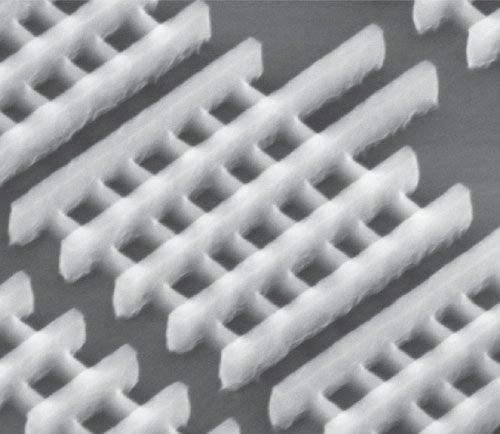
Image courtesy of Intel Corporation.
In the late 1990s, the industry moved toward lowering the wavelength of light sources, using deep ultraviolet laser illumination to achieve a patterning resolution down to 90 nanometers. Combining that wavelength with various optics and other approaches has achieved a minimum resolution of 22 nanometers today. This manufacturing method was used by Intel Corporation to create a new device architecture, called the 3D tri-gate transistor, which is reported to give electrons more space to travel and thus results in higher processor speeds while saving power.
However, the industry is now facing increasing challenges to extend optical lithography beyond this 22-nanometer feature resolution. Proponents of the technology have been working on using extreme ultraviolet wavelengths—13.5 nanometers compared to the current 193 nanometers—as the next step in this downscaling effort. But at this short wavelength, practically all materials will absorb the radiation, so the process needs to use very high power light sources, as well as special masks and optics that will reflect the light and increase efficiency. In turn, suitable resist materials are needed that can withstand such high-power laser exposure. And the entire process needs to happen in a vacuum to minimize absorption losses.
Extreme ultraviolet lithography faces both technical and economic challenges that must be overcome for it to become a viable manufacturing technique to extend optical lithography. Those challenges have directed increasing attention toward nanoimprint lithography as a path forward.
Unlike optical lithography, nanoimprint lithography is essentially a mechanical process, one that relies on direct deformation of the resist to create a pattern. The technique isn’t yet widely used in the semiconductor industry, but has found a niche market in optics, hard disk drives, and biotechnology.
The concept of nanoimprinting has roots as far back as the embossing of metal coins and wax seals in ancient Rome. However, it was Stephen Chou’s group at Princeton University who introduced the term in 1996, and furthered it as a next- generation nanopatterning technique. In 2007, Toshiba validated nanoimprint lithography for device fabrication, and industrial consortiums have since sprung up to drive its research and commercialization.
Hard drives fabricated by nanoimprint lithography may be able to get past the 1 terabyte storage barrier.
The switch from using light to mechanical replication gets around the diffraction limits of light, which bounds the smallest feature size that can be patterned by traditional optical lithography. Nanoimprint lithography also does not require complex and expensive light sources, and the replication process is inherently parallel. It can accommodate a large variety of polymer materials and commercially available resists, and is compatible with either stiff or flexible substrate materials. Such bendy polymer materials easily can be used to create three-dimensional and complex shapes, and the development of roller-printing processes, which Chou proposed in the late 1990s, has significantly advanced the technique’s throughput in the patterning of large areas at low cost. By 1997, the technique was able to reach a resolution of 6 nanometers.
Two variations on the process are currently dominant: thermal nanoimprint lithography (also called hot emboss lithography) and UV-based nanoimprint lithography.
In standard thermal nanoimprint lithography, a heat-responsive polymer is coated onto the substrate. A mold is separately fabricated using semiconductor technologies to create the desired pattern, and is then brought into direct contact with the coated substrate at a controlled elevated temperature and pressure. The imprint temperature is usually at 20 to 50 degrees Celsius above the polymer’s glass transition temperature, making it viscous. The raised pressure drives the polymer to completely fill the cavity features of the mold. The mold and polymer are then cooled while still in contact, so the polymer hardens in the desired shape. The polymer patterns can remain on the substrate for direct use, or can be used as a mask for pattern transfer to the substrate underneath through an etching process.
UV-based nanoimprint lithography operates similarly to the thermal process, except that the resin used is a UV-curable liquid photopolymer, the mold is normally made of optically transparent material (such as quartz), and the entire process can be carried out at room temperature and at slightly lower pressure than the thermal process, but with an added step of exposure to ultraviolet radiation.
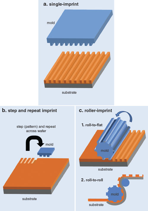
Illustration courtesy of the author.
The nanoimprinting tools used to execute such processes can also be broadly categorized into three different types: single, step-and-repeat, and roller imprint. The earliest tools operated in a single-imprint mode, where the mold patterns must be the same size as the wafer to be patterned. In the step-and-repeat operating mode, the mold patterns a smaller area of the wafer at a time, and then moves to an adjacent area of the unpatterned wafer and repeats the process until the whole wafer is patterned. Hence, the mold in this mode does not need to be the same size as the intended patterned area, a cost saving on a mold that has fine-feature patterning. Although single and step-and-repeat machines allow wafer-based processing, roller-type machines allow continuous (film-based) production. This advance can significantly improve throughput of nanoimprint lithography processes over large areas, and also allows flexible substrates to be patterned. Roller-type machines can be used in either roll-to-flat or roll-to-roll modes.
Optical devices mark one application area that has successfully adopted nanoimprint processes for high-volume manufacturing of products. Two segments of the optics market, wafer level optics and high-brightness light- emitting diodes (LEDs), have springboarded nanoimprinting from R&D into manufacturing reality. In wafer level optics, UV-nanoimprint lithography patterns a lens the full size of a wafer; a multi-lens structure for higher pixel resolution can be made by stacking several full-size patterned wafers together. Compared to conventional processing techniques, this approach offers significant yield and cost advantages and at the same time, allows miniaturization of the optical devices with better performance, made possible through wafer-level patterning.
Over the past few years, explosive growth in the market for high-brightness but low-cost LEDs in display backlighting, signage, general and automotive lighting, and mobile devices, had caused LED manufacturers to turn to nanoimprint lithography to improve the light-emission efficiency of their products while keeping manufacturing costs low. LEDs are produced from compound semiconductor materials (such as gallium nitride). These materials have a high refractive index compared with air, causing much of the light to be trapped inside the LED and leading to poor light emission efficiency. Patterning periodic nanoscale structures with a typical length scale in the range of a few hundred nanometers on the surface of the LED can mitigate these effects and significantly increase its light efficiency and hence its brightness.
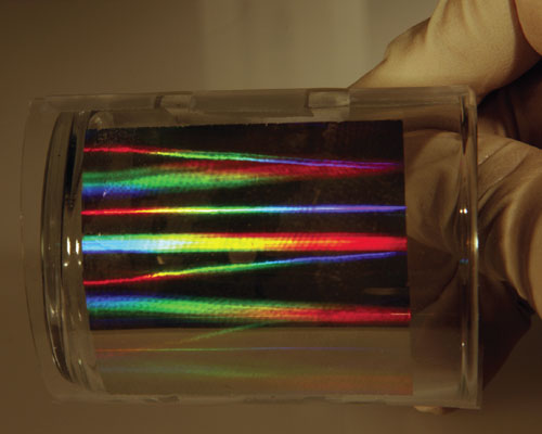
Image courtesy of John A. Rogers, MSE, University of Illinois at Urbana-Champaign.
Conventional optical lithography doesn’t do well in this application, because the inherent waviness of the LED substrate makes it difficult to focus the projected mask. Also, because the length scale is near its optical diffraction limit, the process requires more complex optics and incurs higher costs. On the other hand, UV-nanoimprint lithography provides the advantages of far simpler patterning because it is a mechanical molding process that can easily achieve high resolution. Furthermore, a patterning approach developed by the tool making company Obducat uses a disposable soft polymer stamp replicated from the original hard master stamp, solving the challenge of nanopatterning the nonuniform LED substrate. This solution also increases the lifetime of the expensive master mold, thus making the nanopatterning process highly cost efficient. Commercial manufacturers have reported a capacity of 30 wafers per hour for wafer sizes between 2 and 4 inches, in the production of photonic crystal–based high-brightness LEDs.
Since the 1990s, hard disk drives have been a key application driving the development of nanoimprint lithography from a laboratory technique to commercialization. Demand for hard-drive storage capacity has been growing by about 30 to 40 percent annually in the past few years, particularly with greater use of video and audio applications. However, today’s hard drives are reaching the technical limits of their ability to increase capacity. Conventional drives have randomly placed nanometer-scale grains for recording each bit of data, but there is a threshold size beyond which the grains become increasingly susceptible to thermal fluctuations, which can cause data loss or corruption. Known as the superparamagnetic effect, this phenomenon has posed the primary technical challenge to surpassing conventional drives’ 1 terabyte capacity barrier.
Images courtesy of L. Jay Guo, University of Michigan.
One promising method to circumvent this limitation is to use bit-patterned media. Employing nanoimprint lithography patterning, well-defined and physically separated magnetic nanostructures can be created easily on a single- or double-sided disk surface. Each nanostructure is capable of storing an individual bit. The physically separated bits are less likely to affect their neighbors and thus allow storage of a larger amount of data than conventional hard drives. For example, to reach capacities of 1 terabyte per square-inch or 10 terabytes per square-inch, spacing between the bits of 27 nanometers or 9 nanometers is required, respectively. Nanoimprint lithography is highly capable of patterning these finer features. Furthermore, patterned media do not require multiple layer alignment and are more defect tolerant, making nanoimprinting an adaptable technique for mass manufacturing drives. Major hard drive makers, such as Hitachi Global Storage Technologies, are driving the development of next-generation bit-patterned media drives using nanoimprint lithography.
More generally, nanoimprinting may be a viable technique for fabrication of integrated circuits, especially for flash memory drives. Since 2003, the International Technology Roadmap for Semiconductors—a report issued by an international consortium of industry associations to drive advances in integrated circuit production—has listed the technology as a potential candidate for next-generation lithography for 32, 22, and 11 nanometer nodes, a vote of confidence for its viability. In 2007, Toshiba Semiconductor Company validated it for 22 nanometers and beyond. A simpler nanopatterning process and lower cost have made it an attractive candidate over competing alternative lithography techniques. Throughput has improved from 4 wafers an hour to 20 wafers an hour. Manufacturing defects remain a challenge, but flash memory has built-in redundancy that makes it less vulnerable to such issues.
Nanoimprint technology has wider applications outside of the traditional world of high-tech computing. For instance, biotechnology, a field where medicine and materials meet, has certain applications that are well-suited for the technique. At-home diagnostic devices that use tiny amounts of fluids, such as glucose sensors for diabetics, are often made of disposable plastics, so low per-unit fabrication cost becomes important. Thermal nanoimprint lithography can directly pattern polymers to quickly and cheaply create such devices in a single processing step. In addition, the process can pattern biodegradable and biocompatible materials. Its inherently dry patterning characteristics offer a further advantage, because some biomaterials are susceptible to degradation by solvents, water, or other chemicals, and thus cannot withstand conventional optical lithography’s wet developing process.
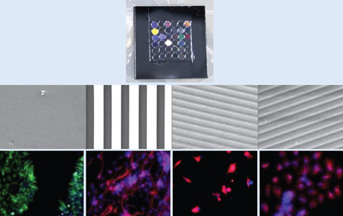
Top photograph courtesy of the author; other images from Ankham et al., 2013, reprinted with permission of Elsevier.
Tissue engineering—which offers a promising alternative for wound repair and organ replacement—is another growing biotechnology domain where nanoimprinting can be employed. A relatively young but important topic is the role that a surface’s topography can have on how cells develop and function. To study this factor, different types of topographies (for example, shapes that are two-dimensional, three- dimensional, micro, nano, curved, anisotropic, isotropic, or have different aspect ratios) have to be manufactured at a large-enough quantity of samples (tens to hundreds) to yield statistically significant results. Thermal nanoimprint lithography can easily create three-dimensional structures from simple two-dimensional molds. A recent demonstration my colleagues and I worked on is a topographical microarray chip called MARC (for multi-architectural chip), which incorporates vastly different topographies onto a single, nanoimprinted surface. One trial of the MARC chip we did with stem cells demonstrates how widely the cells can differentiate simply because of the topology.
Nanofabrication may be useful in biology, but the process can also take inspiration from nature. One mechanism, roller-based continuous processing of materials, has several biomimetic products. This mechanism provides high throughput and also sidesteps the space restriction inherent in using silicon wafers. The roller process works well with flexible substrates, such as plastics, which can create both lightweight and cost-effective products. Initial commercial adopters of the process use it for optical films. Single-layer nanopatterns are directly imprinted onto the plastic film, endowing the material with improved optical performance. Creating functionality directly onto plastics also opens up many opportunities for emerging applications.
One example I have worked on with my colleagues is an antireflection film roller imprinted with nanostructures modeled after the moth eye. Compared to traditional coating-based antireflection surfaces, the nanostructures give these optical films a broader wavelength and wider operating angle while keeping reflectivity at a minimal level.
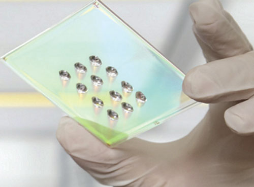
Image reprinted with permission of the American Chemical Society.
Our most recent work takes inspiration from rose petals, which at the nano scale are covered in uniformly distributed conical protusions. Polymers roller-imprinted with similar patterns pin water droplets in place, even when turned upside down. Potential applications include greenhouses, where condensation control is important for healthy plant growth, and dew collection as a source of water in arid regions. In genomics studies, high-quality protein crystals are often grown using hanging drops; nano-imprinted surfaces could increase the yield of such a process by allowing more uniform and controllable droplets.
Some futuristic applications are also on the horizon. Another project my collaborators and I worked on, now being commercialized by the company Nanoveu, patterns lenticular lenses onto plastic film to create a transparent overlay for mobile device screens that creates a 3D image without the need for special glasses. Similarly, groups such as WaveFront Technology are working on depositing a metal grid of nanowires onto films, creating a polarizing effect on the plastic, which can be used in wearable display devices. Roller-type nanoimprinting could be the technology finally to make such long-anticipated products sufficiently affordable, lightweight, and high performance that they could become commonplace.
Click "American Scientist" to access home page

American Scientist Comments and Discussion
To discuss our articles or comment on them, please share them and tag American Scientist on social media platforms. Here are links to our profiles on Twitter, Facebook, and LinkedIn.
If we re-share your post, we will moderate comments/discussion following our comments policy.