Graphene in High-Frequency Electronics
By Keith A. Jenkins
This two-dimensional form of carbon has properties not seen in any other substance
This two-dimensional form of carbon has properties not seen in any other substance

DOI: 10.1511/2012.98.388
The Nobel Prize in Physics for 2010 was awarded jointly to Andre Geim and Konstantin Novoselov of the University of Manchester “for groundbreaking experiments regarding the two-dimensional material graphene.” Essentially it was awarded for the discovery in 2004 of the form of carbon known as graphene, which led to an explosion of experimental and theoretical work with the material around the world. It is remarkable not only that the Nobel Prize was given for the discovery of a material (rather than for the elucidation of some physical principle), but also that the material was already in one of the most common substances in human history, and that the prize was awarded such a short time after the discovery.
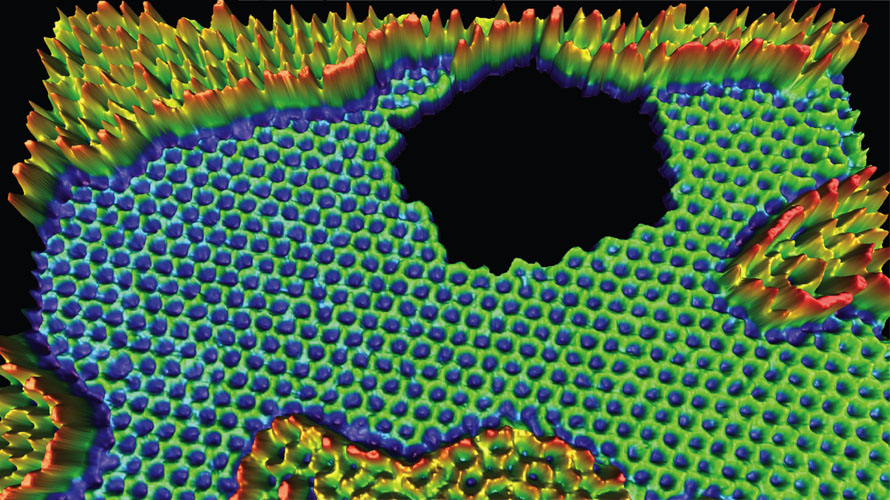
Lawrence Berkeley National Laboratory/Science Photo Library.
In part, the speed of this recognition is due to the amazing excitement created by Geim and Novoselov’s findings. According to Geim, several technical papers are published every day on the subject of graphene. This enthusiasm arose from the quick realization that graphene has many remarkable physical properties not seen in any other material.
What is graphene and what are its properties? It is a two-dimensional form of carbon, a single layer of carbon atoms, in which the atoms are arranged in a hexagonal chicken-wire or honeycomb configuration. It is found in nature and is simply one of the layers of the common substance graphite. Each layer of graphene stacked up to make graphite is only loosely bonded to the others. The layers adhere only by van der Waals forces, weak dipole-to-dipole attractions between adjacent molecules, rather than by stronger covalent bonds, in which the molecules share electrons. This loose bonding explains why graphite is a good lubricant. Technically, graphene was known since x-ray crystallography was able to uncover graphite’s structure in the early 1900s, but it was not isolated into individual planes of graphene until 2004. And there was little interest in graphene by itself until Geim and Novoselov were the first to detail its properties.
Graphene is one of very few two-dimensional materials with a crystalline structure. Its physical layout and electronic properties result in many remarkable characteristics. It is an excellent heat conductor. It is flexible, yet 10 times stronger than any other measured material, at equivalent thicknesses. It is a good absorber of light over a wide spectrum, yet it is effectively transparent. (This dichotomy is not a paradox: A layer of graphene absorbs 2.3 percent of the light impinging on it, which is a lot for a single atomic layer, but still allows most light to pass through.) It is fairly chemically inert, yet when appropriately treated it is a sensitive electrical detector of very small concentrations of chemicals. And it has very high electron mobility, allowing the transit of electrical charges through the material at a rate that is at least 100 times greater, in its purest state, than conventional semiconductors used in electronics, such as silicon or gallium arsenide.
The property of very high electron mobility has excited the electronics community and led to countless predictions. Our apparently insatiable need for speedier computers and greater data throughput in wireless devices has resulted in a universal acceptance that electronic devices and circuits must be made to operate ever faster. The traditional way of achieving this result has been by reducing the size of transistors.
Transistors are made with the class of materials called semiconductors, which conduct electricity under some conditions but prevent its flow in others. That property lets the transistor act as an on/off switch for the binary signals used in computers. The quantum mechanical energy bands that form when atoms are bound together in a crystalline solid make it possible for currents in semiconductors to be carried by both positively charged and negatively charged particles. The negatively charged particles are electrons and the positively charged particles are called holes, implying a place where an electron is missing. Materials that conduct electrons are called n-type (for negative-type) and ones that conduct holes are called p-type (for positive-type). Both n-type and p-type materials can be used in transistors.
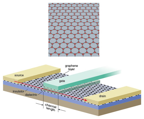
Illustration by Tom Dunne.
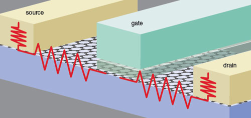
The field-effect transistor (FET) is the most common type used in modern computers. A gate electrode at the center of the device is separated from the semiconductor surface by a thin insulating layer. A current of electrons or holes passing between the FET’s two terminals, called the source and the drain, is controlled by the amount of voltage on the gate. In an n-type FET, for instance, a positive voltage on the gate electrode forms a layer of electrons in the channel region, creating a conducting path in the semiconductor through which current flows.
To speed up a FET, the concept is simple: shorten the distance—the channel length—between the source and drain, and signals will pass between the terminals more quickly. This reduction of dimensions was dubbed scaling by IBM researcher Robert Dennard in the 1970s. (An important side benefit to scaling is that it leads to cramming more transistors into a given area, creating the potential of more functionality on a similarly sized semiconductor.)
However, the difficulty of continuing to reduce the size of conventional silicon-based transistors has caused many to think that the era of scaling is near an end. How can we then make transistors pass signals more quickly? The solution lies in the material of the transistor. Between the source and drain terminals of a transistor is the semiconductor. Although reducing the distance between source and drain increases speed, another way to achieve the same goal is to use a material that conducts electrical signals more rapidly. This aim is why graphene’s mobility is important.
Mobility is a measure of the speed with which electrical signals travel through a material when a voltage is applied. It is easy to see that a material with higher mobility transmits signals faster than one of lower mobility if the dimensions are the same. Compared to other semiconducting materials, silicon actually has a relatively low mobility, but its use is widespread because it has lots of other advantages, such as great mechanical strength and relative ease of manufacture. However, transistors are made from materials that have higher mobility than silicon, such as gallium arsenide (GaAs) and indium phosphide (InP), when they are destined for certain special applications, such as high-frequency wireless transmitters and receivers used in cell phones, or in specialized electronics such as military communications equipment. Graphene transistors may be expected to play a role in these applications because the highest mobility measured for graphene is greater than for the other compounds.
Many scientists and engineers around the world have become excited about the possibility of replacing silicon with graphene to make faster transistors and circuits. Even before graphene’s properties were fully measured or understood, my colleagues and I at IBM, as well as other groups worldwide, believed we should jump right in and try to build transistors and circuits in a way that might lead to technology that could eventually be manufactured just as silicon is used today. The U.S. Defense Advanced Research Projects Agency also believed in this goal and supported this work. Not surprisingly, we encountered many difficulties, but the progress has been very rapid.
Graphite is made of a huge number of sheets of graphene stacked on top of each other. If a single layer of graphite is peeled off, we have graphene. A light pencil mark on paper may actually leave traces of graphene, as pencil “lead” actually contains graphite. But peeling off a single layer of free-standing graphene without having it buckle and fold is not the same as taking a sheet off a stack of paper.
Geim and Novoselov first obtained graphene by exfoliation using transparent tape: By repeatedly sticking the tape on graphite and removing it, they were able to sometimes transfer small flakes of graphene to another carrier material. This technique let them obtain enough graphene to do the seminal experiments that led to their Nobel Prize. This ease of producing graphene probably led to the intense and rapid interest in the material: Any university with a chunk of high-quality graphite, a supply of tape and patient graduate students could produce enough of the material to do some interesting experiments!
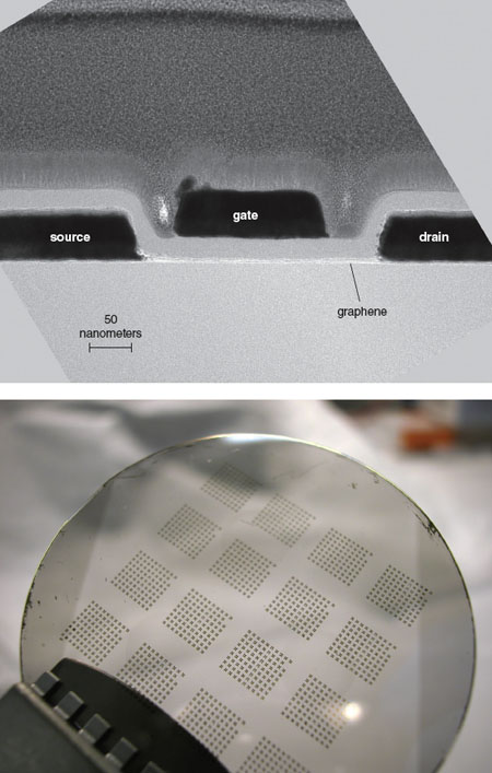
However, the flakes of graphene made this way are tiny: tens of micrometers in width. Such small pieces are enough for experiments but useless for the real electronics applications that our group had in mind. Modern electronic circuits are manufactured by wafer processing: Thin discs with a diameter of 200 or 300 millimeters, made of silicon or other materials, are treated with chemical and optical steps to make dozens or hundred of identical circuits simultaneously. For graphene electronics to be practical, graphene has to be made in larger amounts and sizes, and processed into circuits in a way that can be mass-produced.
At the moment there are two methods of producing graphene on this scale. Both involve processes to grow a single layer of atoms stretching across many centimeters—enormous for this material. Graphene is a picoscale (300 x 10–12 meters) material in one dimension, but macroscopic in its other two dimensions.
Photographs courtesy of the author.
One growth method is the formation of an epitaxial layer (where the crystalline structure of the layer aligns to that of the substrate) of graphene on silicon carbide (SiC). At sufficiently high temperatures the silicon–carbon bonds will break and the silicon will evaporate from the surface, leaving exposed carbon atoms. If this event occurs with appropriate gases present, additional carbon atoms will adhere to those on the surface, forming the hexagonal pattern that makes graphene. This method has been used for a few years to produce 50-millimeter wafers with a silicon-carbide support structure covered completely by a layer of graphene, which can be patterned and formed into devices and circuits using many of the processing techniques found in conventional electronics fabrication. Wafers 100 millimeters in diameter are now becoming available, which makes this method even more attractive. Silicon carbide is particularly useful for radio frequency electronics: Unlike silicon, it is an insulator, so unwanted signals will not propagate from device to device through the substrate. Additionally, it is optically transparent. One drawback of the epitaxial graphene is that one of its surfaces is fairly tightly bonded to the base, impacting its mobility and making for a transistor that would be slower than one made of free-standing graphene.
Another method of producing wafer-scale graphene is growth through the chemical vapor deposition (CVD) of carbon on a catalyst material. Good quality graphene has been produced using copper as the catalyst. If a wafer covered with copper is exposed to ethylene (C2H4) under appropriate conditions, a single layer of graphene forms on it. Of course, copper is a conducting material, and it connects all the graphene together, making it useless for circuits, so the graphene layer must be transferred to an insulating substrate before it can be put into production. The graphene is first coated with a polymer, then the copper on its underside is chemically etched away. The graphene/polymer sheet is placed on a carrier wafer, and the polymer is then removed, leaving a single sheet of carbon atoms. This technique can be used to cover 200- or 300-millimeter wafers with graphene, and any final substrate can be used. Therefore it’s now possible to transfer the graphene onto already-fabricated circuits to make a hybrid technology. The drawback of the CVD method is that, at the moment, the mobility of the graphene is not as high as that formed from epitaxial growth, due to residues of the polymer adhering to the graphene, physical domains (places where the grid of carbon atoms doesn’t align, creating boundaries) and even wrinkles in the graphene sheet. But with the amount of effort spent on generating graphene with CVD, this situation will probably improve.
A transistor made with graphene looks very much like a conventional FET, in that it has a region covered by an insulator under a gate electrode that controls the flow of electrons or holes from source to drain. However, the physical properties of graphene are very different from other semiconductors, and the mechanism of current control is altered, so the electrical properties of a graphene FET diverge quite a lot from conventional FETs.
The most important of these different properties is that graphene does not have a bandgap, an energy range in most nonmetals where electron states cannot exist. In other words, for graphene, as its electrons travel in orbitals around their carbon atoms, there is no energy difference between the conduction band (where electrons are free to move around and form bonds) and the valence band (where electrons are tightly bound to their atoms). Because of this property, some call graphene a gapless semiconductor and some call it a semi-metal. In semiconductor FETs, the bandgap allows the channel to be turned on or off—preventing or allowing a flow of electricity—by applying a voltage to the gate. Without a bandgap, graphene always conducts, but the amount of conduction is controlled by the number of charge carriers in the material. Thus, the current can be modulated, but it cannot be completely stopped. In silicon FETs, the ratio of the on current to the off current might be 1:104 or 1:105, but the ratio for graphene FETs may be smaller than 1:10. Also, in silicon FETs, a state called pinch-off occurs when part of the channel is effectively off, leading to a high resistance to current. High output resistance is required for transistors to amplify the input signal at the gate, which is needed for almost all practical circuits. But the absence of a bandgap in graphene means there is no pinch-off in its channel region, so achieving high output resistance is difficult.
Because silicon FETs can be turned off, they can be used for digital computers for which there are only two states allowed: on or off, current flowing or current blocked. In standard silicon-manufacturing technology, most of the transistors are off most of the time. With millions of transistors in an integrated circuit, this means the current flow is controllable. If the off-state of such transistors only resulted in a small reduction of current, then the circuits would require enormous amounts of power to keep them going, and we would never have home computers or portable electronic devices, because they would heat up and deplete their batteries very quickly. However, analog and radio frequency circuits, which modulate the amplitude of signals rather than turn them on or off digitally, are essentially always conducting. Silicon FETs can be used for digital or analog circuits, but graphene FETs are better suited—at the moment—just for analog circuits.
There are some other interesting differences between graphene and semiconductors. Because it is a purely two-dimensional material, it has no body, no bulk. All current flows on its surface. As a result, anything contacting graphene might affect its current flow by scattering it off the atoms of the contacting material. Additionally, in semiconductors the level of gate voltage required to turn the transistor on has been controlled by adding small amounts of other materials, in a process called doping. But doping in graphene is only possible through surface contact, which again is hard to control during manufacturing.
Finally, current sometimes flows equally well in both directions through a graphene FET. In silicon and other semiconductors with a bandgap, current is predominantly via either electrons or holes, as determined by the fabrication of the transistor. But graphene allows almost equal conduction of electrons and holes, so it is an ambipolar device. (However, when the graphene is made from silicon carbide, it becomes unipolar.) So far, this property is regarded as a nuisance, but there might be some unique applications resulting from this quirk. There have been demonstrations of frequency multipliers and dual-mode amplifiers (both used with communications signals) that make use of this peculiar property.
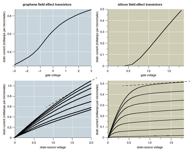
The result of these different behaviors can be seen in traditional direct-current (DC) electrical characteristics of the graphene FETs. The transfer characteristic relates the output current through the drain to the input voltage on the gate, from which transconductance is derived. Qualitatively this measurement shows how “strong” the device is: A stronger device delivers more current for a given input voltage than a weaker device. The output characteristic relates the drain current to the drain voltage, from which the output resistance is computed. Both transconductance and output resistance of any transistor need to be known to design analog circuits.
Yet in spite of the very different physics and resulting DC electrical behavior, it has been shown that graphene FETs behave very much like their semiconductor counterparts when they are operated at high frequency, under alternating-current (AC) conditions. This comparison is made by measuring each system’s frequency response, its output signal strength when it is given a particular input signal.
The primary means of estimating frequency response is through the cutoff frequency. A universally used metric for describing the frequency response of FETs, cutoff frequency is a fundamental property indicating how quickly a signal can travel from the gate to the drain of the device, and all new device technologies are measured against both existing ones and projections of expected cutoff frequencies in the future.
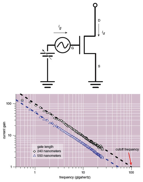
This metric is derived from other measurements that describe the frequency dependence of the small-signal AC current gain of a transistor when the output is short-circuited. An AC voltage is applied to the gate at various frequencies, resulting in an AC input current. The measured output current (also AC) is divided by the input current, as a function of frequency. In the case of FETs, this only makes sense for AC measurements, as no DC current can flow through the insulating gate. If a FET is well behaved, this current gain should decrease as the inverse of the frequency. The point at which it falls to a value of 1 is the cutoff frequency.
Some of our earliest work with graphene FETs, which were actually made from tiny flakes of the material, showed the right AC behavior. The current gain drops with frequency, so “cutoff frequency” is a meaningful term. Additionally, cutoff frequency was shown to be proportional to the transconductance divided by gate capacitance, and cutoff frequency increased as the channel length was reduced. These three traits showed that in high-frequency operation, graphene FETs act a lot like semiconductor FETs, which nurtured the idea that graphene transistors could potentially be used in similar circuits. In a few short years, we have seen cutoff frequency increase from a few gigahertz to over 300 gigahertz, almost catching up with the most sophisticated semiconductor devices.
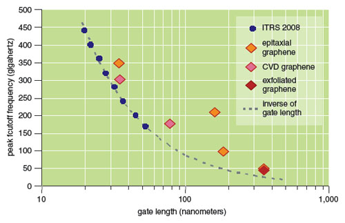
Frequency response depends inversely on the length of the gate, and proportionally to the transconductance, which is loosely proportional to mobility. Thus, to make faster devices, we can either reduce the gate length or use higher mobility materials. The work with graphene has consistently shown the advantage of its mobility. Compared to silicon FETs, graphene FETs have always had higher cutoff frequencies at the same gate length.
Transistors are one of the building blocks of electronic circuits, but unless they are connected, they don’t have any useful function. Prior to the 1960s, transistors were connected to other electronic components—resistors, capacitors, other transistors and so on—by wires, then made into items such as radios and televisions. Then the era of modern electronics started, with the invention of the monolithic integrated circuit, in which all these components were fabricated together on a single substrate, eliminating bulky wiring, which led to miniaturization and a tremendous increase in function and variety. All of today’s radios, phones and computers are made this way.
With that in mind, our team at IBM decided to start work on an integrated graphene circuit, while also developing improved graphene transistors. We realized we shouldn’t wait until the transistors were perfect before we tried to make a circuit with them. The transistor is fairly simple compared to a circuit with interconnections and other components. We knew that in the process of developing an integrated circuit, we would uncover problems that were better faced as soon as possible, and we were eager to start.
The idea of the integrated circuit is that most or all of the circuit is built on the same substrate, using many steps to deposit and pattern layers of materials to create the required components. These steps are repeated on many locations on a wafer, yielding a large number of identical circuits produced on a single substrate. In semiconductor technology, these processes are numerous and very sophisticated. However, applying these steps to a wafer covered with graphene turned out to be challenging for several reasons. First, graphene has poor adhesion with the metals and oxides used in integrated circuits. Because the graphene layer is only a single atom thick, it is vulnerable to damage by some of the common etching processes. In addition, the substrate materials and dielectrics employed in the experimental graphene transistors were not all suitable for wafer-scale fabrication. Finally, the integrated circuit required a mixture of thick and thin metal layers, which requires different processing.
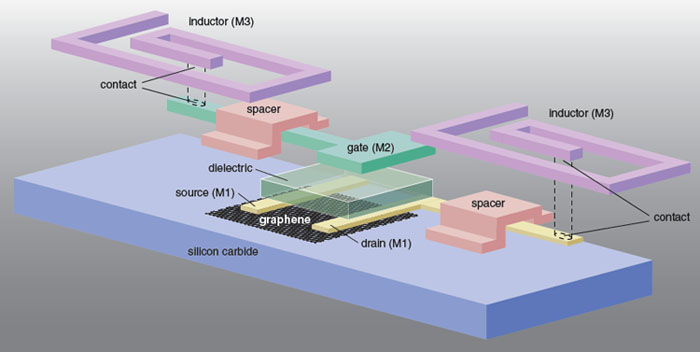
Illustration by Tom Dunne.
Discovering and then solving these problems took almost a year. More than 60 processing steps were required to make this integrated circuit, 5 or 10 times more than the number required to make a wafer full of single graphene transistors. The circuit was made from a silicon carbide wafer covered with epitaxially grown graphene. The result was a frequency mixer. The area of the circuit is less than 1 square millimeter. Although it uses only one FET, it is a sophisticated combination of devices, interconnectors, insulators and inductors.
Frequency mixers are at the heart of almost every wireless communication circuit, and they are required for a signal-detection principle of radio tuning invented by Columbia University electrical engineer Edwin Armstrong decades before transistors were developed. If we imagine building wireless electronics from graphene, a mixer is a very important circuit to use as a starting point. Mixers combine two signals of different frequencies, the radio frequency (RF) signal that carries the information over a long distance, and the local oscillator (LO) signal, which is used to convert the signal to a frequency that is usable by the receiver. The mixer produces a signal composed of the difference in frequencies of these two inputs (it also produces a sum signal, but this is actually an undesired by-product). If the input frequencies are of close value, then the difference between the two is quite low and might, for example, be in the audio range, even if the input signals are orders of magnitude higher than human hearing range.
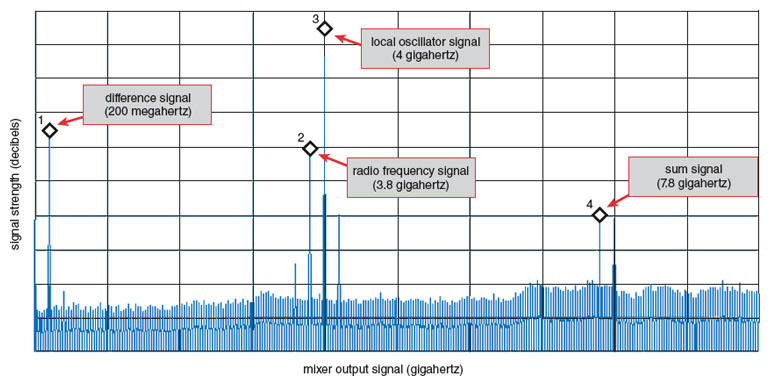
The successful operation of the graphene mixer is illustrated in Figure 8, which shows a frequency spectrum of the output signal. The two inputs, the RF signal and the LO signal, are seen at 3.8 gigahertz and 4.0 gigahertz, respectively; as required by mixing, the difference signal is seen with a value of 200 megahertz. The unwanted sum signal is also present, but its amplitude is much suppressed by the impedance of an inductor in the output path. We made other measurements to validate the correct operation, with the conclusion that this graphene mixer is quite successful. It has a rather large signal loss, which is undesirable, but our experiments have shown us what we need to do to improve this outcome. Its level of integration is actually greater than some conventional mixers operating at similar frequency. Testing the mixer also gave us a pleasant surprise: It operates almost unchanged over a temperature range from 300 kelvin to 400 kelvin. Most conventional RF semiconductor circuits require additional feedback circuitry to enable operation over wide temperatures. In separate work done by our group at IBM, it has been found that graphene devices have a frequency response that is almost unchanged to a very low temperature of 4.3 kelvin, so it appears that graphene electronics has the very attractive property of being temperature-independent over a huge range.
Our graphene device has not been perfected. Some “amplifiers” actually attenuate signals instead, and the integrated mixer has a rather large signal loss. Although tremendous progress in exploiting graphene for RF circuits has been made in a very short time—just four years—there is still a lot to be done before it is ready to replace any existing technologies.
One major challenge is to preserve graphene’s mobility. Pure graphene has a mobility that is 10 or more times higher than silicon, yet the cutoff frequencies seem to be running at only two times the values of silicon FETs at the same dimensions. This discrepancy results from graphene being all surface. When it is suspended, free of contact on both sides, it has high mobility. When something touches it, its mobility usually drops considerably, as the charge carriers (electrons and holes) scatter off the adjacent materials on their way through the graphene. Part of the problem comes from the substrate on which the graphene is grown or placed. Also, to make a gated device, there must be a dielectric (an insulator that can be polarized by an electric field) between the gate and the graphene. So a graphene FET inevitably has contact with materials that can rob it of some of its potential. There is considerable engineering effort to reduce the impact of contact by finding different materials and by altering the physical structure of the devices. If the mobility of free-standing graphene can be retained in a full transistor structure, it will be a tremendous leap ahead in electronics performance.
The physical device structure is presently limiting performance as well. The issue is resistance: Any resistance in the path from source to drain causes a reduction in transconductance, even if the graphene mobility is high. There are two locations in graphene devices with high resistance. One is at the contact between the metal electrodes and the graphene itself. Because of the chemical and quantum mechanical properties of graphene, this resistance is usually large, but there is work being done to see if it can be reduced. Its not known yet if this is a fundamental problem or “just” an engineering problem. The second source of resistance is the region between the gate graphene and the source and drain contacts, called the access region. Even though this is a fairly small distance, ungated graphene is of high resistance. It’s as if part of the gate is not doing its job of turning the channel on. This is an engineering problem. Using the technique called self-alignment, which automatically creates a gate that almost fills the region between source and drain, it should be possible to greatly reduce the length of the access region, thereby reducing this unwanted resistance.
Output conductance is also a problem and can be seen in the output characteristic. The ideal FET has an output that is flat above a certain drain voltage, which is equivalent to an infinite differential output resistance. A small change of the gate voltage of a transistor causes a change in its drain current. If the output resistance is infinite, this current will flow to the load attached to the transistor—such as an external resistor or another transistor—which results in voltage or power amplification of the gate voltage. This amplification, or gain, is required for almost all electronic components; otherwise, the signal applied to the circuit will be attenuated and eventually lost. If the transistor, however, has a finite output resistance, some of the current modulated by the gate will be dissipated in the transistor and hence not transferred to the load. If too much of the current is lost in the transistor, there will be loss instead of gain, and the device will be useless. Graphene FETs tend to have rather poor output resistance when the gate lengths are small, so this problem is serious for graphene. If the channel is long, drain current saturation is seen, which is equivalent to high output resistance, but a long channel device has low frequency performance, and therefore may not be practical. Getting short-channel graphene FETs to saturate is challenging. There has been some recent progress based on very thin gate dielectrics, which basically improves the transconductance. Using a thin dielectric can also improve the drain current saturation. There’s a lot left to be done, but some devices with gain have been demonstrated, and it looks like there is a path to improvement.
Like any analog circuit, graphene FETs have to face a problem of noise. All analog signals have unwanted noise: If it is too large, it masks or corrupts the transmitted signal. If noise is present at the input to an amplifier chain, it will be amplified along with the signal of interest; if there is noise added by the devices in the amplifier chain, there will be a net increase of noise at the output. At the moment we simply don’t know if graphene makes a low-noise transistor, but perhaps it has lower noise than conventional semiconductors. Based on its conduction mechanism, many people believe it will be superior, but the experiments just haven’t been done yet.
What if we can extend the electrical performance of graphene a bit more so it becomes as good as silicon, or even a little better? Then how might it be used? One interesting possibility is to combine graphene circuits with some other technology, such as conventional semiconductor circuitry, to exploit the best of each. A layer of graphene circuits might be placed on a patterned semiconductor wafer. The graphene layer can be used for analog and RF circuits, while the semiconductor part can be used for digital processing of the RF signals. A hybrid technology like this seems feasible now that we are able to transfer a single layer of CVD-grown graphene onto any substrate, including one that has been processed to contain circuits.
Looking further, we are considering some other attractive graphene properties. It is almost transparent, it absorbs light, it is flexible and strong and it works over a wide temperature range. Circuits made from graphene might be used for invisible electronics, such as on windows or glasses; for flexible circuits, for example, sewn into clothing; or for circuits to be used in extreme temperature environments, such as space and underground exploration. Although separate electronics may already exist for these situations, perhaps only graphene can be of use in these circumstances with the extra advantage of very high-frequency operation.
Click "American Scientist" to access home page

American Scientist Comments and Discussion
To discuss our articles or comment on them, please share them and tag American Scientist on social media platforms. Here are links to our profiles on Twitter, Facebook, and LinkedIn.
If we re-share your post, we will moderate comments/discussion following our comments policy.